Intel started talking about the Ponte Vecchio in 2019, when Raja Koduri first talked about Intel Xe-HPC, the version of its GPUs for the high-performance computing market. The development of this graphics processor is linked to the Cray Aurora supercomputer. Now, two years later, they have completed their design and talked for the first time about its power, 1 PetaFLOP for Intel Xe-HPC Ponte Vecchio.
It has been years since Raja Koduri left AMD to join Intel. His goal? Create his most ambitious design to date, which is the Ponte Vecchio. A design that builds on the unique strengths of Intel that would not have been possible in its previous company, AMD. After two years in the design phase, this GPU is already a reality.
Intel Ponte Vecchio, the most ambitious GPU in history
Peta-flops in your palm. An ambitious dream. @intel
Silicon engineers and our packaging alchemists achieved it in just 2 years! @pgelsingerInfectious Energy for Technology is a great accelerator for our forward march to bring this magic to a cloud near you. pic.twitter.com/C4LMuNrY2F– Raja Koduri (aRajaontheedge) March 24, 2021
Raja Koduri, Intel’s current chief graphics architect, after leaving AMD for two years to join Intel, has finally unveiled what we might consider his most ambitious work to date. The GPU for high performance computing Ponte Vecchio, also known as the Intel Xe-HPC, and made it from his own Twitter account.
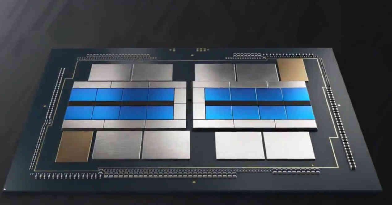
Ponte Vecchio is made up of two monolithic GPU chips, each internally made up of 8 Xe-HPC tiles and 8 Rambo Cache tiles. All this mounted on an interposer with 8 HBM2 memory chips divided into 4 chips per GPU. To all this we have to add two Xe-Base classified chips, of which at the moment we do not know what their functionality is.
All of this in an integrated circuit with over 100,000 million total transistors under Intel’s 7nm node, indicating that we are dealing with a chip of massive size and enormous complexity.
Intel comes to PetaFLOP on a GPU before everyone else

A PetaFLOP is 1000 TeraFLOPS, and this is the number that Intel reached with Ponte Vecchio, but it should be noted that they achieved it thanks to specialized units for artificial intelligence, which are analogous to the Tensor Cores of NVIDIA and whose inclusion in the Xe- The HPC was already confirmed since 2019.
It should be noted that the Xe-HPC will not compete in the PC graphics card market, but against the NVIDIA Tesla based on the A100 GPU and against the AMD CDNA. In the case of the A100, the floating point power through its measurement cores is 312 TFLOPS in FP16, which is three times the power. For all this we can not forget that Ponte Vecchio are two monolithic chips and that it uses 2 chips instead of one.
The launch of the Ponte Vecchio is expected in 2022, when NVIDIA is expected to launch the successor to its current A100, it is not known how NVIDIA will react. What we can guess from Raja’s video is that the size of the Ponte Vecchio is massive and much larger even than the NVIDIA A100s.
Who will manufacture Ponte Vecchio, Intel or TSMC?

The information we have so far is that the Ponte Vecchio will be manufactured by Intel, as the design uses Intel’s EMIB and Foveros technologies. This contrasts with the information that other Intel Xe designs will be created by TSMC, especially the Intel Xe-HPG gaming graphics cards.
It’s worth noting that Intel’s 7nm build node is not equivalent to TSMC’s 7nm, since the build nodes no longer correspond to any metrics, but rather to the Intel node that the Ponte Vecchio will be built on. It is equivalent to TSMC’s 5nm node.
The fact that Intel has completed the design and Raja shows the finished chip is an important message from Intel, as they not only show that their 7nm node is up and running to make chips, but can make circuits highly integrated as well. Something that for Intel is extremely important to demonstrate its strength in the future market, which depends on the strength of its 7nm node.